
Atomically thin transistors promise smaller electronics, but shrinking a switch is only useful if electricity can still get into it properly.
That deceptively simple problem sits at the centre of a KAIST-led study highlighted on 16 September 2026. The researchers used tin diselenide as a shared charge injector for two kinds of atomically thin semiconductor. The underlying paper appeared in Advanced Materials on 12 August, so the September news is a fresh explanation of earlier published research. Research paper
The appeal is easy to understand: a future chip may contain extraordinary switching materials, yet still lose much of their advantage at the point where those materials connect to the rest of the circuit.
Why atomically thin transistors struggle at the contact
Modern digital circuits pair two transistor types. One carries current through electrons; the other uses holes, which behave like positive charge carriers. Together they enable complementary switching, commonly called CMOS.
Ultrathin materials are attractive because their active layers can be extremely thin. However, depositing a conventional metal contact can damage those layers, while the resulting interface can resist the flow of charge. A contact that works well for one transistor type may not suit the other. KAIST’s explanation, distributed through Tech Xplore
This is a useful reminder about chip development. A promising material has to work with everything touching it. Laboratory excellence in isolation does not automatically survive the connections needed to build a circuit.
One material, two routes for current

The researchers paired their injector with tungsten diselenide and molybdenum disulfide channels. Its interfaces enabled charge to tunnel through barriers by different mechanisms. They also demonstrated an inverter, a basic circuit that turns a high input into a low output and vice versa.
One result was more than a thousandfold improvement in drive current over the conventional metal-contact comparison for the p-type device. That is a result for a particular transistor and comparison—not a thousandfold faster processor, or a measured saving in an AI data centre. Advanced Materials
The hard part comes after the elegant result
KAIST points to further work on direct growth, larger-area fabrication and integration before such materials could support densely stacked circuits. The prospect is to put more useful electronics into a given footprint; the study does not announce a commercial processor or a manufacturing launch. KAIST
For the industry, the next convincing evidence would be consistency across many devices, compatibility with production steps and useful behaviour in more complex circuits. A spectacular result in a carefully prepared sample is a starting point for those questions.
The interesting competitive story therefore sits below familiar brand names. Future progress will depend on engineers solving problems that rarely appear on a product box. Getting electricity cleanly into a layer only atoms thick is one of them.
Related reading: the wider race to build AI computing systems.
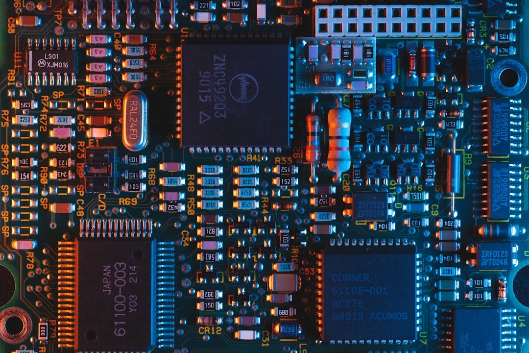
Featured image: Circuit-board components illustrate the electronics context; this is not the experimental KAIST device.
Leave a Reply