
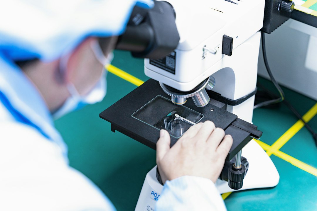
Featured image: Engineers testing optical hardware illustrate semiconductor and networking production work. Contextual photograph; not visual evidence of the specific development. Photo: Lightsaber Collection via Unsplash. Unsplash licence.
The visible symbol of the AI build-out is a GPU. The harder industrial problem is everything required to turn designed silicon into a working rack. On 21 October 2026, Nvidia announced new agreements covering chip substrates, advanced packaging, testing and optical engines, with capacity targets extending through 2028.
The announcement is a map of potential bottlenecks rather than a report that all new capacity exists today. Supplier agreements, reservation payments and production targets can make expansion more likely. They cannot guarantee factory qualification, yield, schedule or final accelerator deliveries.
A GPU depends on layers that rarely appear in the product name
Advanced accelerators combine multiple dies, high-bandwidth memory and complex interconnects. Substrates provide the fine electrical pathways between packaged chips and circuit boards. Interposers connect dies and memory at very high density. Packaging assembles those components, and testing identifies faults before expensive systems reach customers.
Nvidia says agreements with IBIDEN, Samsung Electro-Mechanics and Unimicron are intended to increase aggregate substrate supply by 2.5 times over three years. “Aggregate” matters: it combines capacity across suppliers and does not state that every vendor or every product line grows at the same rate.
The company also says Amkor plans to increase advanced-packaging interposer-wafer capacity by more than 300% by the end of 2028. A percentage can look dramatic when the starting base is not disclosed. The useful follow-up metrics will be qualified wafer output, yield and the number of finished packages supported.
Testing capacity gets money before it gets volume
Nvidia expects total testing capacity to double across 2026 and 2027. It announced a $1.1 billion capacity-reservation advance to King Yuan Electronics Company for new US facilities, with high-volume manufacturing targeted for April 2027. A separate Singapore site is targeted for February 2027.
A reservation advance helps a supplier justify equipment and construction for expected demand. It is neither a purchase of $1.1 billion of completed chips nor a guarantee that the line reaches its planned volume on time. Semiconductor facilities must install tools, train staff, qualify processes and achieve acceptable yields.
The Wall Street Journal’s report on the announcement placed the agreements in the broader race to expand chipmaking capacity. The competitive context is real, but company projections remain forward-looking statements rather than audited production outcomes.
Optical engines reveal the networking constraint
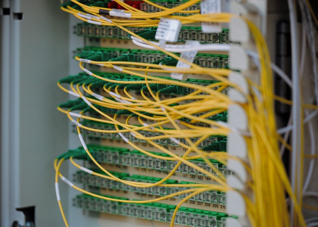
Modern AI systems need accelerators to exchange enormous amounts of data. Electrical links become harder to scale in bandwidth, distance and power, pushing optical connections closer to the computing package. Co-packaged optics places optical components near switching silicon to reduce electrical reach.
Nvidia says Siliconware Precision Industries plans to increase optical-engine capacity for co-packaged optics by 15 times by mid-2027 and then double it again by the end of 2028. Those targets signal that networking components, not only compute dies, are central to planned AI-factory scale.
Optical manufacturing brings its own yield, alignment, thermal and reliability problems. A capacity target does not show that every product has passed qualification or that customers have deployed it in volume.
Diversification reduces one risk and creates coordination work
Multiple substrate vendors and geographically distributed test sites can reduce dependence on a single facility. They also require consistent specifications, quality control, logistics and traceability across more partners. A weak link can constrain the number of complete systems even when other components are abundant.
The announcement therefore should not be converted directly into future GPU shipments or data-centre revenue. Demand, electricity connections, cooling, memory supply and customer financing could change before the new lines mature.
Nvidia’s plan is significant because it makes the hidden production stack unusually visible and commits capital to several layers at once. The next evidence will arrive in factory milestones: installed tools, qualified processes, volume output and delivered systems. Until then, the multipliers describe intended capacity—not hardware already serving an AI model.
Reporting and source checks completed on 22 October 2026. By FutureTechDose Editor.
Leave a Reply